高通验证 HBC 堆叠内存,AI250 2027 年送样
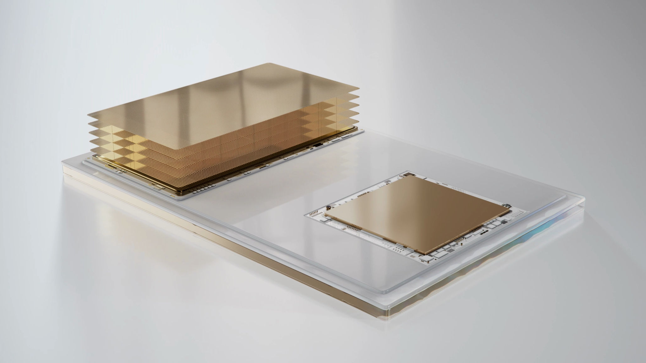
高通(Qualcomm)今早宣布,已完成其高带宽计算(High Bandwidth Compute,HBC)内存架构的初步验证,该架构将成为公司即将推出的 Dragonfly 数据中心 AI 加速器的核心组成部分。这种堆叠式内存架构将让高通及其制造合作伙伴把多层 DRAM 堆叠在一颗小型计算芯片之上,从而让内存更靠近访问它的计算硬件,使高通得以从更紧密的硬件布局中获得能效与成本效益上的收益。
此次技术验证的完成,使 HBC 距离在商业产品中部署又近了一步,相关产品计划于明年开始送样。高通现已验证该技术可行,并且其能效与内存带宽接近预期水平,这使其能够在明年推进量产,同时让客户(及投资者)持续了解高通 Dragonfly AI250 加速器及其后续产品的开发进展。
高通 HBC:以近存计算减少数据搬运
HBC 最早在高通 2026 年投资者日上公布,是一项由高通主导的新技术,旨在利用近存计算(near-memory compute)在内存容量、内存性能与生产成本之间建立新的平衡——高通希望在这三个方面都实现突破。
从根本上说,该技术是 HBM 及其他内存堆叠技术的进一步变体。但与 HBM 不同的是——HBM 将多颗 DRAM 芯片堆叠在一颗基础芯片(base die)之上,再通过超宽内存总线连接回主处理器——HBC 则力图省去中间环节,转而把一颗小型计算芯片置于堆叠结构的底部。
Qualcomm HBC 加速器示意图(Solid)
理论上,把内存放置在计算裸片之上有若干好处。其中最大的一点是能效,因为搬移数据需要消耗能量——而把大量数据搬移较长距离会消耗更多能量。通过把内存放置在计算裸片之上,连 HBM 连接这段相对较短的距离也被消除(更不用说 LPDDR5X 这类外部内存),从而把搬移数据所消耗的能量降到最低。这些节省下来的能量又可以反过来用于提升芯片本身的性能,或是在相同的能耗足迹内容纳更多芯片组成集群。
计算裸片本身并不是一颗完整的处理器。但通过把最消耗内存带宽的操作放在该裸片上,再把结果回传给处理器中央那颗更大的计算裸片,Qualcomm 试图让内存与计算硬件尽可能贴近。
Qualcomm HBC 与 HBM 对比(Solid)
Qualcomm 的这一努力同样着眼于生产成本。由于 HBM 使用宽内存总线,需要 CoWoS 或 EMIB 等先进封装才能将 HBM 堆栈连接到计算裸片和内存控制器。而通过把大部分计算负载转移到位于内存下方的计算裸片上,将该计算裸片与芯片封装上其他位置更大的处理器裸片连接起来所需的带宽就少得多。因此,这条连接可以用成本更低的技术来构建,例如传统的 2D 有机基板。
Qualcomm HBC 与 HBM 对比详解
话虽如此,HBC 并没有消除所有复杂性。与 HBM 一样,它仍然需要使用 TSV 将多个 DRAM 裸片(在高通的方案中则是晶圆)键合在另一颗裸片之上,这本身就是一项具有挑战性的工艺。这意味着对复杂制造技术的需求并未消失,只是从存储器堆叠和高速 chiplet 互连两者,缩减到仅剩存储器堆叠。
最后,高通希望在此实现内存带宽与内存容量之间更好的平衡。值得注意的是,该公司的 HBC 设计采用 LPDDR5X DRAM 裸片,而非 HBM 所用的薄型高性能裸片。该公司尚未说明该技术最终的性能表现,但一个 HBC 堆栈的容量预计已经超过当前 HBM4 实现所能达到的水平。
高通 HBC 对比 HBM 对比 SRAM
高通在这一切背后的根本论点是,HBC 比任何其他内存架构都提供了更全面的解决方案,无论是 HBM、片上 SRAM 还是封装外 LPDDR。按其提出的方案,HBC 相对这些技术各有优劣,但正如高通所主张的,它们能够实现远超外部 LPDDR——并接近 HBM——的内存带宽(进而带来性能),同时既没有使用片上 SRAM 的容量限制,也没有这两种方案中后者的高成本。
归根结底,这一切旨在让高通能够打造出更好的 AI 推理芯片,以比现有技术更少的短板满足推理对内存带宽和容量的需求。
验证 HBC:双堆栈测试发现每瓦带宽达到 HBM4 的 5 倍
深入验证流程本身,在首次 HBC 验证中,Qualcomm 将一套早期的 HBC 样品堆叠连接到了其圣地亚哥实验室里的一台测试设备上。
Qualcomm HBC ATE 测试台
这套测试装置本身并不起眼,但其中装着一颗对 Qualcomm 而言至关重要的芯片,关系到其数据中心计划。
鉴于这是早期样品,需要指出的是,他们在这里测试的 HBC 堆叠只有 2 层 DRAM 裸片。量产产品将有 4 层。因此 Qualcomm 尚未进入测试全尺寸堆叠的阶段。
Qualcomm HBC 验证:我们如何测量
Qualcomm 简要介绍了其验证方法:他们将 HBC 测试堆叠与自动化测试机配合使用,通过该测试机既以 LPDDR5X 器件的身份、也以 HBC 器件的身份对该堆叠进行测量。
Qualcomm HBC 验证结果
最终,Qualcomm 在其成功的验证测试中得出三项主要发现。第一项当然是这套方案确实能跑通,证明其可行。在性能方面,Qualcomm 测得自家 HBC 方案的能效(以每瓦带宽计)比 HBM4 按其自身规格所标称的水平高出五倍以上。最后,虽然该公司没有披露具体带宽数字,但他们将测得的带宽归类为外部 LPDDR5X 的 18 倍。
尤其是能效数据,略低于 Qualcomm 对该技术最初的预期——他们原本希望能比 HBM 高出 6 倍。但如果这一表现能延续到完整产品上,它仍代表着能效的显著提升。
据 Qualcomm 称,其验证测试还包括产品的热行为,不过该公司并未就此提供更多细节。到目前为止,Qualcomm 对该话题鲜有表态,但散热考量是他们需要克服的主要技术障碍之一,因为在堆叠存储架构中,作为基础裸片的计算裸片更为活跃,预计会产生更多热量。
随着初步的 HBC 验证完成,Qualcomm 目前正考虑推进该技术商业化的下一步,即其 Dragonfly AI250 加速器。作为今年将推出的 Dragonfly AI200 加速器的后续产品,AI250 将是首款集成 HBC 的产品——此后它也将成为 Qualcomm 未来 AI 加速器的关键组成部分。AI250 尚未确定发布日期,但据 Qualcomm 称,它将于明年上半年开始送样,这可能意味着该公司计划有所提前——此前最初宣布的送样时间是 2027 年年中。
如果 HBC 一切进展顺利,该技术也不会仅限于 Dragonfly AI 加速器。Qualcomm 此前曾宣布,他们还将把该技术引入面向消费者的 Snapdragon 产品——不过该公司当时并未具体说明时间以及哪些产品。
归根结底,HBC 对 Qualcomm 来说是一项旨在提高能效、降低 TCO 的举措。如果这项技术成功,Qualcomm 预计能够交付比当代设计更节能、制造成本也更低的 AI 推理加速器。这反过来又会使其在大规模 AI 推理运营中,运营成本低于 GPU(理想情况下,采购成本也更低)。未来几个月,随着 Qualcomm 准备在明年上半年对 Dragonfly AI250 送样,我们将看到这一前景如何发展。
译文由英文原文机器翻译,术语按行业惯例统一,可在文末展开原文核对。
查看英文原文(Qualcomm Validates HBC Stacked Memory Ahead of 2027 Dragonfly AI250 Sampling)
Qualcomm Validates HBC Stacked Memory Ahead of 2027 Dragonfly AI250 Sampling - ServeTheHome
HomeServerAcceleratorsQualcomm Validates HBC Stacked Memory Ahead of 2027 Dragonfly AI250 Sampling
Qualcomm this morning is announcing that it has completed the initial validation of its High Bandwidth Compute (HBC) memory architecture, which will be a central part of the company’s upcoming Dragonfly data center AI accelerators. The stacked memory architecture will see Qualcomm and its manufacturing partners place multiple layers of DRAM on top of a small compute die in order to bring memory even closer to the compute hardware that is accessing it, allowing Qualcomm to reap the energy efficiency and cost efficiency benefits of a closer hardware placement.
The recent validation of the technology moves HBC one step closer to deployment in commercial products, which are scheduled to start sampling next year. Qualcomm has now validated that the technology works and is delivering energy efficiency and memory bandwidth close to their expectations, allowing them to move towards mass production next year while keeping customers (and investors) in the loop on the development of Qualcomm’s Dragonfly AI250 accelerator and its successors.
Qualcomm HBC: Near Memory Compute for Less Data Movement
First announced by Qualcomm back at their 2026 Investor Day, HBC is a new Qualcomm-spearheaded technology that is intending to use near-memory compute in order to strike a new balance between memory capacity, memory performance, and production costs – with Qualcomm looking to push the envelope on all three aspects.
Fundamentally, the technology is a further variation on HBM and other memory stacking technologies. But unlike HBM where multiple DRAM dies are stacked on top of a base die that is connected back to the host processor over an ultra-wide memory bus, HBC aims to cut out the middleman by placing a small compute die at the bottom of the stack instead.
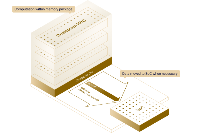 Qualcomm HBC Accelerator Diagram Solid
In principle, placing memory on top of a compute die has several benefits. The biggest of these is energy efficiency, as moving data around costs energy – and moving large amounts of data large distances costs even more energy. By placing memory on top of a compute die, this eliminates even the relatively short distance of an HBM connection (to say nothing of external memory like LPDDR5X), minimizing the amount of energy spent to move that data around. Those energy savings, in turn, can be funneled back into improving performance of the chip itself, or allowing a larger number of chips to be clustered together within the same energy footprint.
The compute die itself is not a full processor. But by placing the most memory bandwidth-intensive operations on the die and then sending the results from that back to the larger compute die at the center of the processor, Qualcomm is looking to get their memory and compute hardware as close together as is feasible.
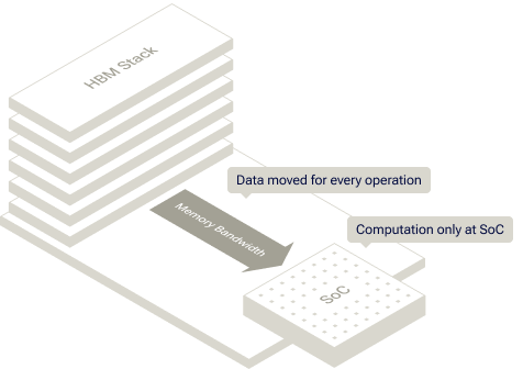 Qualcomm HBC Compared to HBM Solid
Qualcomm’s efforts are also eyeing production costs here. Because of the wide memory bus used by HBM, it requires advanced packaging such as CoWoS or EMIB to connect HBM stacks to a compute die and memory controllers. But by shifting most of the computational workload to the compute die that sits under the memory, far less bandwidth is needed to connect the compute die to a larger processor die elsewhere on the chip package. And, consequently, that connection can be built with cheaper technologies such as traditional 2D organic substrates.
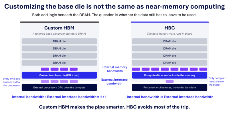 Qualcomm HBC vs HBM Detailed
That said, HBC does not eliminate all of the complexity. Like HBM, it still requires bonding multiple DRAM dies (or in Qualcomm’s case: wafers) on top of another die using TSVs, which is itself a challenging process. Which means the need for complex manufacturing techniques has not gone away, but it has been reduced from both memory stacking and high speed chiplet connectivity to just the memory stacking.
Finally, Qualcomm is looking to strike a better balance between memory bandwidth and memory capacity here. Notably, the company’s HBC design calls for using LPDDR5X DRAM dies rather than the thin, high-performance dies used by HBM. The company has not outlined what the final performance of the technology will be, but the capacity of an HBC stack is already projected to be larger than what current HBM4 implementations can achieve.
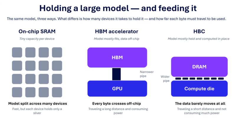 Qualcomm HBC vs HBM vs SRAM
Qualcomm’s fundamental argument through all of this is that HBC provides a better all-around solution than any other memory architecture, be it HBM, on-die SRAM, or off-package LPDDR. As proposed, HBC has strengths and weaknesses versus all of these technologies, but as Qualcomm argues, they can achieve memory bandwidth (and thus performance) far better than external LPDDR – and approaching HBM – without the capacity constraints of using on-die SRAM, or the high costs of the latter of those two solutions.
Ultimately, all of this is meant to lead to allowing Qualcomm to build a better chip for AI inference by meeting inference’s need for memory bandwidth and capacity with fewer drawbacks than existing technologies.
Validating HBC: 2 Stack Test Finds 5x Bandwidth-per-Watt of HBM4
Diving into the validation process itself, for their initial HBC validation Qualcomm has hooked up an early HBC sample stack to a test unit in their San Diego labs.
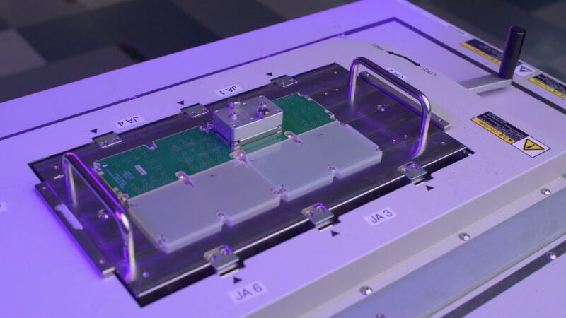 Qualcomm HBC ATE Test Rig
While the test setup itself is not much to look at, inside of it is a chip that, for Qualcomm, is critical to their data center plans.
Given that this was an early sample, it should be noted that HBC stack they were working with here just had 2 layers of DRAM dies. Shipping products will have 4 layers. So Qualcomm is not yet at the point where they are testing full-sized stacks.
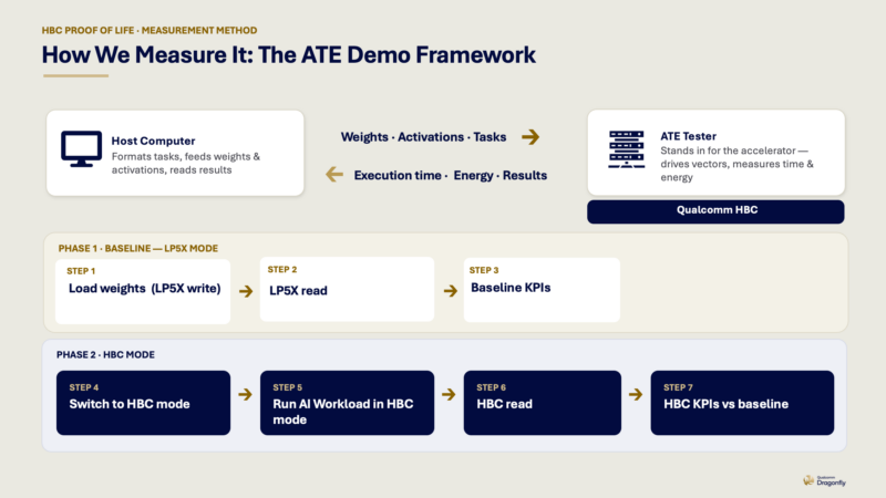 Qualcomm HBC Validaiton How We Measure It
Briefly outlining their validation approach, Qualcomm tells us that they used the HBC test stack with an automated tester, which was used to measure the stack as both an LPDDR5X device and as an HBC device.
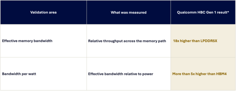 Qualcomm HBC Validation Findings
Ultimately, Qualcomm had three major findings with their successful validation testing. The first, of course, being that this worked at all, proving that it can be done. Meanwhile in regards to performance, Qualcomm measured their HBC solution as delivering more than five-times the energy efficiency (on a bandwidth-per-watt basis) than HBM4 as per its own specifications. Finally, while the company is not disclosing specific bandwidth figures, they are categorizing the measured bandwidth at 18x higher than external LPDDR5X.
The energy efficiency figure in particular is a bit short of Qualcomm’s initial projections for the technology, where they were hoping to beat HBM by 6x. But if this carries over to a full product, it still represents a significant improvement in efficiency.
According to Qualcomm, their validation testing also includes the thermal behaviors of the product, though the company has not gone into any further detail there. Qualcomm has had little to say on the subject so far, but thermal considerations are one of the major technical hurdles they will need to overcome, as a more active compute die as the base die in a stacked memory architecture is expected to put out more heat.
With their initial HBC validation complete, Qualcomm is now looking at moving on to the next step of commercialization of the technology with their Dragonfly AI250 accelerator. The successor to the Dragonfly AI200 accelerator due this year, AI250 will be the first product to integrate HBC – and it will be a key part of future Qualcomm AI accelerators after that. AI250 does not have a launch date yet, but according to Qualcomm it will begin sampling in H1 of next year, which is potentially a move-up for the company’s plans following the initial announcement that sampling would take place in the middle of 2027.
If everything pans out with HBC, the technology will not be limited to Dragonfly AI accelerators, either. Qualcomm has previously announced that they would also be bringing the technology to their consumer-focused Snapdragon products – though the company is not specifying when and what products at the time.
Ultimately, HBC is a play for energy efficiency and a lower TCO for Qualcomm. If the technology pans out, the company expects to be able to deliver AI inference accelerators that are both more energy efficient and cheaper to build than contemporary designs. Which in turn would make them cheaper to operate (and ideally, cheaper to acquire) than GPUs for large AI inference operations. We will get to see how that plays out over the coming months as Qualcomm moves towards sampling Dragonfly AI250 in the first half of next year.
原文为英文,正文由自动抓取并保留原文。
原文发布于 ServeTheHome(Qualcomm Validates HBC Stacked Memory Ahead of 2027 Dragonfly AI250 Sampling),标题、摘要与正文由机器翻译,术语按行业惯例统一,未经人工逐句校订。


