AI正在改变晶圆厂运作方式,工程师因此提速
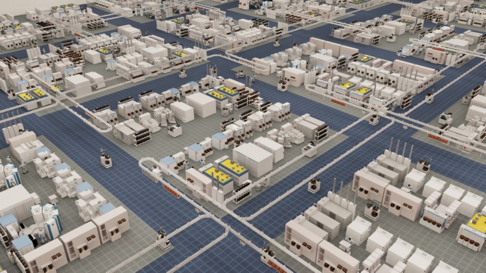
先进芯片的需求正在上升。制造这些芯片的工艺正变得越来越复杂。而容错空间正在不断缩小。
对工程师而言,理解工艺变更会如何表现、某种材料与新增工序将如何相互作用、缺陷如何追溯到根本原因,是半导体制造中关键且充满挑战的环节——而这些分析可能耗时数天。在晶圆厂产线上进行物理实验既慢又贵。在良率或工艺质量上判断失误,会带来实实在在的后果。
AI 正在改变半导体制造,影响着工程师能做什么——以及能做多快。
加速计算缩短了仿真时间,让工程师在投入物理试验之前能够评估更多备选方案。
基于物理的 AI 帮助工程师预测工艺表现,而无需每次都运行完整仿真。
AI 智能体可以处理过去要耗费数小时的系列工程任务。
数字孪生则让团队能在虚拟环境中测试变更,然后再投入物理试验。
这些能力共同描绘出一个 AI 定义的晶圆厂:在这样的半导体制造工厂里,AI 帮助工程师优化工艺、更早发现问题,并在芯片制造的完整生命周期中做出更好的决策。工程师主导工作,凭借自身专业知识做出判断,同时花更少时间等待答案。
加速计算不只是加快单项计算的速度——它还改变了工程师在最终决定前能测试多少种方案。
多物理场仿真用于建模热传递、电学行为和机械应力等物理效应之间的相互作用。
借助 NVIDIA cuDSS 库,多物理场仿真软件供应商 COMSOL 正将此类面向半导体制造的仿真加速最高 10 倍。这有助于工程师优化设备和工艺、比较不同方案,并决定哪些改动需要做实物测试。
Applied Materials 与 NVIDIA 正在合作,加速原子尺度的材料发现与工艺开发。通过集成 NVIDIA cuDSS,Applied 的 Ginestra 仿真平台运行速度比仅用 CPU 的方案快最高 10 倍。而借助 NVIDIA PhysicsNeMo,Applied 的 ACE+ 多物理场平台将形貌仿真提速最高 35 倍。
在某些情况下,加速不只是缩短计算时间——它让计算本身成为可能。计算光刻——即决定电路图形如何印制到硅片上的过程——涉及的计算量极大,在生产规模下用 CPU 无法完成。Siemens 正在将 NVIDIA cuLitho 集成到其 Calibre 光刻软件中,在关键仿真工作负载上实现最高 17 倍加速。这拓展了工程师在晶圆进入曝光工序前所能验证的范围。
因此,更快的计算有助于研究人员探索影响下一代半导体工艺的材料行为和反应路径。
除了加速仿真之外,基于物理规律训练的 AI 还能预测材料和工艺的表现——无需每次都运行完整的仿真。
这种收益在那些即便使用加速硬件也十分昂贵的复杂计算中体现得最为明显。
等离子体——半导体刻蚀工艺中使用的带电气体的——就是一个例子。对等离子体行为进行建模,需要求解能够刻画电学、化学与热学过程如何相互作用的方程,这使得反复仿真成本高昂。NVIDIA PhysicsNeMo 可以帮助将等离子体预测仿真时间从数天缩短到最短几毫秒。
Lam Research 打算将 NanoVDB 集成到其先进的半导体工艺建模平台 SEMulator3D 中,该平台隶属于该公司虚拟产品系列 Semiverse Solutions。加入 NanoVDB 后,预计可将部分晶圆刻蚀建模加速最高 30 倍。
工程师将分析转化为决策——修改设计、排查测试失败、调整生产工艺等等。
AI 智能体可以帮助完成这些决策之间的各个步骤。
评估某项给定任务该采用哪个 AI 模型就是一个例子:这是一个串行的人工流程,在测试现场可能耗费数小时。
Advantest 正在使用 NVIDIA NeMo Switchyard AI 智能体来自动完成这一选择,将响应时间从数小时缩短到几分钟。
数字孪生让团队能够在虚拟环境中模拟设备配置、布局和工艺变更,然后再投入实体试验。这降低了实验成本,尤其是在晶圆厂日益复杂、错误变更代价越来越高的情况下。
Applied Materials 使用 NVIDIA Omniverse 库为整座晶圆厂构建物理精确的数字孪生。团队可以模拟物料流动、识别瓶颈、评估布局与运营策略——将虚拟实验从单个工艺扩展到整座工厂的运转方式。
半导体制造的未来在于把这些能力连接起来:用生产数据为模型提供输入,用模型评估变更,再把评估结论反馈给做生产决策的工程师。
这正是 AI 定义的晶圆厂所承诺的图景:AI 帮助人们从每一个生产周期中学习,并更快地依据这些知识采取行动。
了解 NVIDIA 如何与半导体行业领军企业合作,覆盖芯片的全生命周期。
译文由英文原文机器翻译,术语按行业惯例统一,可在文末展开原文核对。
查看英文原文(AI Is Changing How Semiconductor Fabs Work — and Engineers Are Moving Faster Because of It)
Demand for advanced chips is rising. The processes to build them are getting more complex. And the margin for error is shrinking.
For engineers, understanding how a process change will behave, how a material will interact with a new step, how a defect maps back to a root cause are critical, challenging steps in semiconductor manufacturing — and these analyses can take days. Physical experiments on a fab line are slow and expensive. A wrong call on yield or process quality has real consequences.
AI is transforming semiconductor manufacturing, impacting what engineers can do — and how fast.
Accelerated computing shortens simulation time, allowing engineers to evaluate more alternatives before committing to physical trials.
Physics-based AI helps engineers predict process behavior without running a full simulation every time.
AI agents handle sequences of engineering tasks that once consumed hours.
And digital twins let teams test changes in a virtual environment before committing to physical trials.
Together, these capabilities describe an AI-defined fab: a semiconductor manufacturing factory where AI helps engineers optimize processes, catch problems earlier and make better decisions across the full manufacturing chip lifecycle. Engineers direct the work and make decisions based on their expertise while spending less time waiting for answers.
Shorter Simulation Cycles Change What Engineers Can Explore
Accelerated computing doesn’t just speed up individual calculations — it changes how many alternatives engineers can test before committing.
Multiphysics simulations model interactions among physical effects, such as heat transfer, electrical behavior and mechanical stress.
Using the NVIDIA cuDSS library, multiphysics simulation software provider COMSOL is accelerating such simulations for semiconductor manufacturing by up to 10x. This helps engineers optimize equipment and processes, compare alternatives and decide which changes to test physically.
Applied Materials and NVIDIA are collaborating to accelerate atomic-scale materials discovery and process development. By integrating NVIDIA cuDSS, Applied’s Ginestra simulation platform runs up to 10x faster than CPU-only approaches. And with NVIDIA PhysicsNeMo, Applied’s ACE+ multiphysics platform delivers topography simulations up to 35x faster.
In some cases, acceleration doesn’t just shorten the calculation — it enables it altogether. Computational lithography — which defines how circuit patterns are printed onto silicon — involves calculations too intensive to complete on CPU at production scale. Siemens is integrating NVIDIA cuLitho into its Calibre lithography software, delivering up to 17x acceleration on key simulation workloads. That expands what engineers can verify before a wafer goes to print.
As such, faster calculations can help researchers explore material behavior and reaction pathways that influence next-generation semiconductor processes.
Predicting Process Behavior Without Running Every Simulation
In addition to accelerating simulations, AI trained on physics can predict how materials and processes will behave — without running a full simulation each time.
The payoff is most visible in complex calculations that are expensive even on accelerated hardware.
Plasma — the electrically charged gas used in semiconductor etch processes — is one example. Modeling plasma behavior requires solving equations that capture how electrical, chemical and thermal processes interact, making repeated simulation costly. NVIDIA PhysicsNeMo can assist in reducing plasma-prediction simulation time from days to as little as milliseconds.
Lam Research intends to integrate NanoVDB into its advanced semiconductor process modeling platform SEMulator3D, part of the company’s Semiverse Solutions family of virtual products. The addition of NanoVDB is expected to accelerate select wafer-etch modeling by up to 30x.
Agents Handle the Steps Between Decisions
Engineers turn analyses into decisions — revising a design, investigating a test failure, adjusting a production process and more.
AI agents can help carry out the steps between those decisions.
Evaluating which AI model to apply to a given task is one example: a sequential, manual process that can consume hours on the test floor.
Advantest is using NVIDIA NeMo Switchyard AI agents to automate that selection, reducing response times from hours to minutes.
Testing Factory Changes Before They Reach the Line
Digital twins let teams simulate equipment configurations, layouts and process changes in a virtual environment before committing to physical trials. This reduces experimentation costs, especially as fabs become more complex and the stakes of a wrong change get higher.
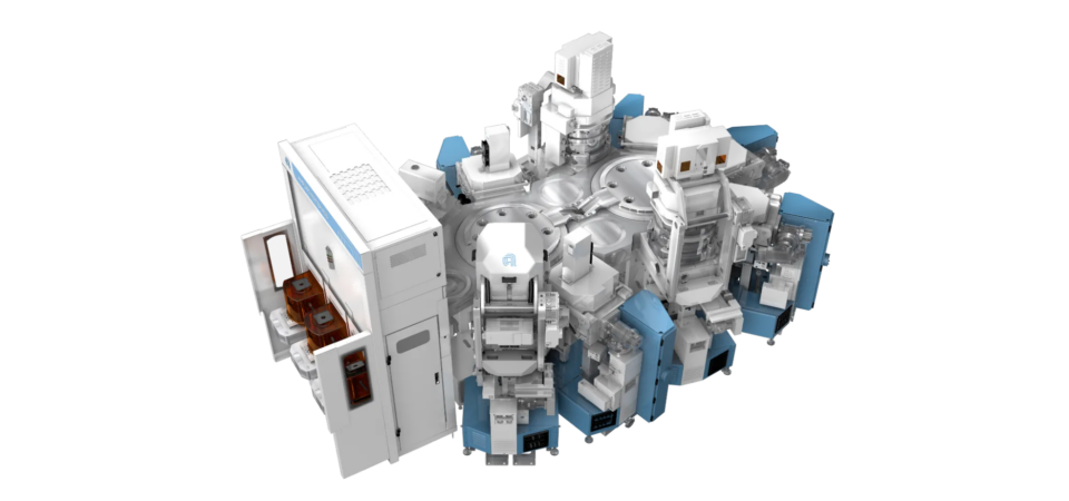
Applied Materials uses NVIDIA Omniverse libraries to build physically accurate digital twins of entire fabs. Teams can simulate material movement, identify bottlenecks and evaluate layouts and operating strategies — extending virtual experimentation beyond individual processes to how the factory works as a whole.
The Connected Loop
The future of semiconductor manufacturing lies in connecting these capabilities: using production data to inform models and models to evaluate changes, then bringing those findings back to the engineers making production decisions.
That’s the promise of the AI-defined fab: where AI helps people learn from each production cycle and act on that knowledge sooner.
Explore how NVIDIA is working with semiconductor leaders across the chip lifecycle.
正文保留英文原文,标题与摘要由机器翻译。
原文发布于 NVIDIA Blog(AI Is Changing How Semiconductor Fabs Work — and Engineers Are Moving Faster Because of It),标题、摘要与正文由机器翻译,术语按行业惯例统一,未经人工逐句校订。
