2500美元8GB矿卡电压毛刺破解成A100 80GB

有志于构建自己本地 AI 集群的技术爱好者,有远比购买 DGX Sparks 或 Apple Mac Studios 更有趣的选择。二手数据中心 GPU 随处可见,服务器机架里的垃圾对爱好者来说就是宝藏。随着 CMPunlocker 的出现,这一选择变得更受欢迎;它是针对 Nvidia CMP-170HX 卡的软改,可解锁远超原厂状态的能力。现在,一位技术人员更进一步,通过电压毛刺突破了剩余限制,打造出一张比实际售价 20,000 美元、配备 80GB VRAM 的 Nvidia A100 GPU 还快的卡……但它来自一张 2,500 美元的 8GB CMP-170HX 矿卡。
桌面 GPU 路线图;Nvidia 企业级 GPU 路线图;用 GPU 解压测试 DirectStorage;GeForce RTX 30 系列升级矩阵——你的 Ampere GPU 在 2026 年需要升级吗?;Rubin 深度解析;The Stout Owl:终极 Noctua G2 PC
这项电压改装由 Kate 完成(GitHub 链接见此处),她的起点来自一篇论文,该论文描述了如何利用 GA100 卡的微码。她将注意力转向通常受保护的板载熔丝控制器。尽管很少被讨论,但一段时间以来,几乎任何 CPU 和 GPU 中都少不了“熔丝盒”——不过它通常只在工厂使用一次,用于断开芯片中测试不佳部分的物理连接,从而禁用它们,以便作为低端型号出售。
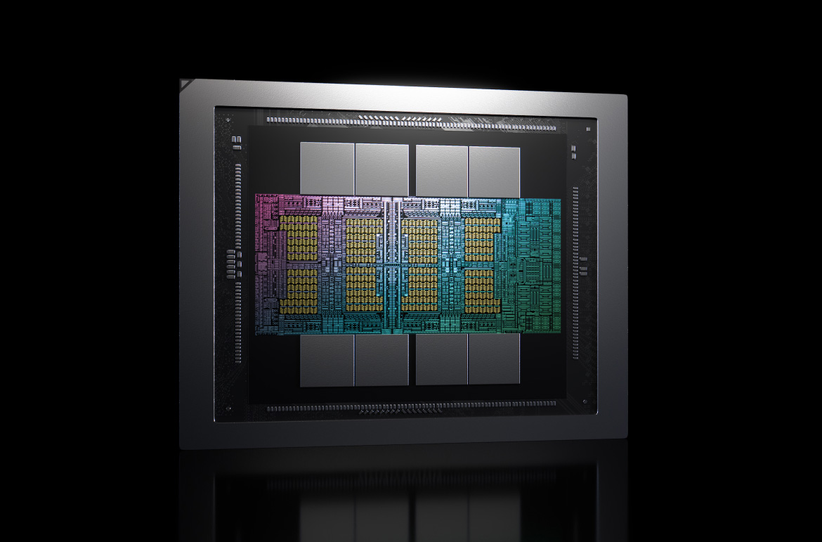
如果你想知道人们如何从 8-10GB 中获得 80-40GB 的 VRAM,解释很简单:GA100 芯片实际上内部包含所有对应的 HBM2e 显存裸片;但它们在工厂被像着色器模块一样禁用。较小的版本更受欢迎,因为它基于内部配有 80GB HBM2e 的 GA100 变体,而 10GB 卡则来自 40GB 的 GA100。
这里说的 Nvidia 显卡配备了一个相当精巧的 eFuse 控制器(512 x 32 阵列中共 16,384 个)——可以通过读取它来获取显卡当前的配置。显卡的几乎每个部分都有对应的熔断丝:VRAM 区域、各个着色器模块、PCIe 4.0 和 NVLink,甚至视频编解码硬件。然而,正如 Kate 简洁地指出的:Nvidia 的设计并不安全,因为烧断熔断丝反而能解锁更多功能,而不是更少。
正常情况下,用户无法烧断或"写入"这些熔断丝——但一个拿着烙铁的极客可不是普通用户。Kate 让 GPT-6 Astra 设计了一块基于 8 美元 STM32G4 微控制器的简单电路板,用来接入显卡 PCB 上的电源信号。
显卡上的电压调节器(VRM)"说"的是 PWMVID——这是 Nvidia 的一项标准,而 Kate 的电路板截获了发送给 VRM 控制器的 PWM 信号,迫使它在向 GPU 供电的线路上产生电压毛刺,而熔断丝控制器正位于这条线路上。
还记得我们说过熔断丝控制器是只读的吗?借助电压毛刺,以及在紧密循环中大量读取熔断丝状态,她成功把控制器置入了一种状态,使其安全位标志允许写入通过。从那一刻起,重新配置她的显卡就"很容易"了。她非常谨慎地强制禁用了此前被标记为有缺陷的着色器模块,因为这些是物理熔断丝——没有"撤销"按钮。
她将改装应用到了自己的显卡上,在用多种工作负载测试后,发现其中九张的 80 GB 显存全部可用,而有一张卡"只有"64 GB 可用。最有趣的是,解锁所有着色器模块(SM)后,她的 FP16 FMA 性能比普通 A100 显卡高出 20%。她认为这是因为这些芯片往往有 120 个或更多可用 SM——超过规格表上的 108 个。GA100 裸片初始就设计了 128 个 SM,以应对缺陷,这在芯片制造中很正常。
在驱动上启用这些"新"功能必须使用 CMPUnlocker 软件改装,但它并不能释放显卡的全部潜力:显存上限为 40–64GB(取决于版本),许多着色器模块仍处于锁定状态,PCIe 带宽也只到 2.0。此外,它不支持 ECC、NVLink 或多实例 GPU,而这些在服务器部署中都至关重要,也用于产品分级。
Kate 的电压改装打破了所有这些限制,她最好的一张测试卡以 PCIe 4.0 速率稳定运行,且功能齐全。她没有测试视频编码器部分,但使用这些显卡的人不太可能太在意这一点。
至于成本,CMP-170HX 8GB 目前价格在 3,000 美元左右,10GB 版本约为 2,500 美元。满血版 Nvidia A100 80GB 的 PCIe 配置可达 20,000 美元甚至更高。SXM 服务器模块版本更便宜,但需要配套基础设施。请注意,这些价格可能会有很大波动,尤其是随着越来越多人了解到这些改装。
Kate 说,她现在公布自己的研究,是因为另一个人独立发现了同样的问题。她已将这一漏洞告知 Nvidia,不过对于已经上市的在售显卡,该公司能做的并不多。
译文由英文原文机器翻译,术语按行业惯例统一,可在文末展开原文核对。
查看英文原文(Techie uses voltage glitching hack to turn $2,500 Nvidia 8GB cryptomining GPU into a full-fat $20,000 A100 with 80GB of VRAM)
Enterprising techies looking to build their own local AI cluster have far more interesting options than buying DGX Sparks or Apple Mac Studios. Used data center GPUs are everywhere, and a server rack's garbage is an enthusiast's treasure. This option has become even more popular with CMPunlocker, a soft-mod for Nvidia CMP-170HX cards that unlocks abilities well beyond stock. Now, a techie has taken it a step further, blasting through the remaining limitations with voltage glitching and creating a card faster than the actual $20,000 Nvidia A100 GPU with 80GB of VRAM... but from an $2,500 8GB CMP-170HX mining card.
The volt-mod was done by Kate (GitHub link here), who got her starting point from a paper that described how one could exploit GA100 cards' microcode. She turned her attention to the normally protected onboard fuse controller. Although it's rarely discussed, a "fuse box" has been integral in most any CPU and GPU for a while — though it's normally used once at the factory to break physical connections in chips to parts that have tested poorly, thus disabling them so they can be sold as a lower-end model.
If you're wondering how people are getting 80-40GB of VRAM out of 8-10GB, the explanation is simple: the GA100 silicon actually includes all the corresponding HBM2e VRAM dies within; but they get disabled at the factory like the shader modules. The smaller version is more desirable, as it's based on the variant of GA100 with 80GB of HBM2e within, while the 10GB cards spawn from the 40GB GA100.
The Nvidia cards in question have quite an elaborate eFuse controller (16,384 in a 512 x 32 array) — which can be read to obtain the card's current configuration. Most every part of the card has related fuses: VRAM sections, individual shader modules, PCIe 4.0 and NVLink, and even video codec hardware. However, as Kate succinctly put it: Nvidia's design is insecure, as popping fuses can grant access to more features, not fewer.
Under normal conditions, these fuses can't be popped, or "written to," by the user — but a geek armed with a soldering iron isn't a normal user. Kate had GPT-6 Astra design a simple circuit board based on an $8 STM32G4 microcontroller to tap into the power signals on the card's PCB.
The voltage regulators (VRMs) on the card "speak" PWMVID, an Nvidia standard, and Kate's board intercepted the PWM signals sent into the VRM controller, forcing it to produce voltage glitches on the line feeding the GPU, where the fuse controller lies.
Remember when we said the fuse controller was read-only? With the voltage glitches, many fuse-status reads in a tight loop, and she managed to set the controller to a state in which its security bit flags allowed writes through. From that point, it was "easy" to reconfigure her card. She was careful to force-disable any shader modules previously marked as defective, because these are physical fuses — there's no "undo" button.
She applied the mod to her cards and, after testing with multiple workloads, found that nine had the full 80 GB of VRAM working, and one card "only" had 64 GB usable. Most interestingly, unlocking all the shader modules (SM) nets her FP16 FMA performance 20% beyond a regular A100 card. She thinks this is due to the chips often having 120 or more usable SMs — over the 108 on the spec sheet. The GA100 die starts with 128 SMs to account for defects, which is normal in chip manufacturing.
The CMPUnlocker soft mod is required for enabling the "new" features on the drivers, but it doesn't unlock the card's full potential: the VRAM upper limit is 40-64GB (depending on the variant), many shader modules remain locked, and PCIe bandwidth only goes to 2.0. Additionally, there's no ECC, NVLink, or multi-instance GPU support, all of which are critical in a server setup and are also used for product segmentation.
Kate's volt-mod does away with all of these limits, and her best test card is happily working at PCIe 4.0 speed with the full feature set. She didn't test the video encoder bits, but it's unlikely anybody using these cards cares much for that.
As for the cost, a CMP-170HX 8GB is currently hovering around $3,000, and the 10GB variant costs around $2,500. A full-fat Nvidia A100 80GB in a PCIe configuration can reach $20,000 or more. The SXM server-module versions are cheaper, but they require infrastructure around them. Note that these prices will likely vary significantly, especially as people become increasingly aware of the mods.
Kate says she's publishing her research now because another person independently found the same issue. She has informed Nvidia of the vulnerability, though there's not much the company can do for existing cards already on the market.
正文保留英文原文,标题与摘要由机器翻译。
原文发布于 Tom's Hardware(Techie uses voltage glitching hack to turn $2,500 Nvidia 8GB cryptomining GPU into a full-fat $20,000 A100 with 80GB of VRAM),标题、摘要与正文由机器翻译,术语按行业惯例统一,未经人工逐句校订。