AMD Venice-X 达 5.3 GHz,3D V-Cache 重返数据中心
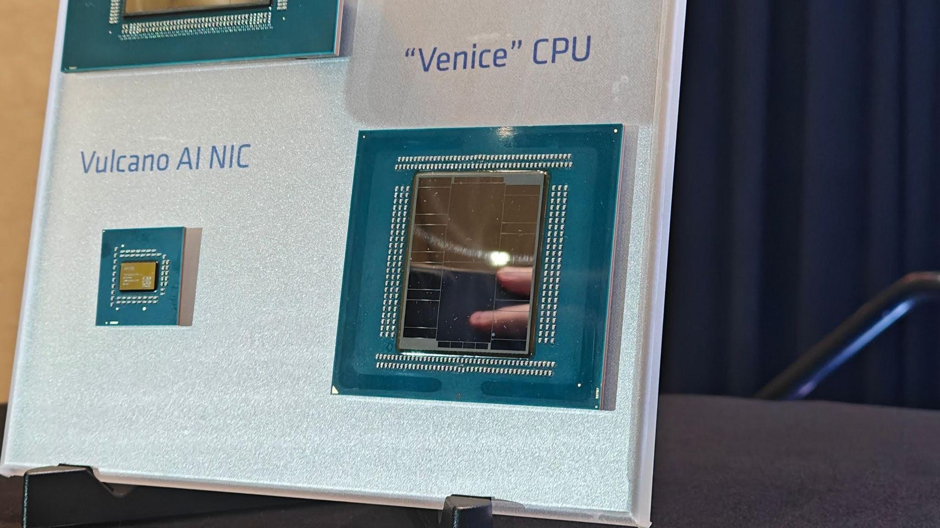
AMD在上一代未能推出Turin-X CPU,这使得其3D V-Cache技术在2023年Genoa-X发布后,于数据中心领域中断了四年。明年下半年,3D V-Cache将随Venice-X重返HPC,其96核与1,152 MB L3缓存与EPYC 9684X(Genoa-X)持平,但时钟频率大幅提升,支持PCIe 6.0,单插槽内存带宽接近此前的四倍。
AMD于2022年通过Milan-X首次将混合键合引入EPYC处理器,一年多后又推出了Genoa-X。Turin一代过去,没有一款芯片采用堆叠SRAM,但如今它随Venice-X回归。这一次的关键变化并非来自核心数——以及随之而来的缓存——的大幅提升,标准SP7产品线才是如此。真正的关键是5.3 GHz的加速时钟频率,这同样是整个Venice系列的支柱之一,而它对Venice-X所瞄准的HPC工作负载尤为有利。
核心数 / 线程数
基础 / 加速时钟频率(GHz)
EPYC 9006X(SKU未知)
未知(可能为400至600 W)
从以往几代顶级的EPYC -X芯片可以看出,X系列芯片的加速频率明显更低,而各代产品中频率更高的则是标准版芯片。Milan最高可扩展至4.1 GHz,Genoa则可攀升至4.4 GHz,但EPYC -X芯片并非如此。Venice-X则带来了整个产品线中最高的5.3 GHz加速频率,将高频率与大规模键合L3缓存统一起来,服务于HPC工作负载。
关于 Venice-X 仍有细节缺失,包括基础频率、产品线中有多少款 SKU 及其规格,以及 TDP(不过其他 Venice CPU 可用的 400 至 600 W 区间很可能是其范围)。不过,这些芯片似乎采用 SP7 插槽,与此前的 EPYC-X 芯片保持一致。
该平台提供 96 条 PCIe 6.0 通道,而面向企业的较小规模 SP8 平台则以内存通道换取 PCIe 通道。Venice-X 具备 SP7 上完整的 16 通道内存配置,包括对 12,800 MT/s 的 MRDIMM 的支持,可实现其标称的每插槽 1.6 TB/s 内存带宽。
据 AMD 称,Venice-X 面向 HPC 工作负载的关键结合点在于高频率与大容量堆叠缓存的搭配。AMD 目前在其 HPC 集群中同时保留 3D V-Cache 和高频 EPYC 芯片,用于运行其内部的 EDA 工作负载。AMD Fellow Phil Steinke 表示,公司对这些工作负载进行性能分析,以刻画性能特征、优化 EPYC 设计,并推动合作伙伴优化其软件。
据 Steinke 称,HPC 集群上迄今为止最大的消耗者是功能验证工作负载,占 AMD 所用算力的一半以上。这些是出现在 Cadence Xcelium 等工具中的逻辑仿真,Steinke 表示 EPYC 团队“全年 7×24 小时”运行这些工作负载。
上图为其中一类工作负载的示例,使用 AMD 的 uProf 监控工具测量 IPC。AMD 称,借助 3D V-Cache,该工作负载完成速度提升 40%,每时钟指令数约为原来的两倍。AMD 未说明其比较的是哪些芯片或使用的是什么应用。不过,该对比是在配备与未配备 3D V-Cache 的 EPYC 集群之间进行的。
Steinke 表示,AMD 如今能够借助 Venice-X 迈向单芯片方案,在功能验证等工作负载中保持缓存优势,同时更好地支撑对频率更为敏感的 EDA 负载。Steinke 说:“我提到过,我们的数据中心里混用着高频 CPU 和 3D V-Cache CPU,这是因为从 Milan 到 Genoa,高频型号在频率方面始终略高一些。”“有了 Venice-X,这种割裂就不存在了。你可以在单颗 CPU 上兼得两者之长,这正是我们非常期待将其用于自身业务的一点。”
AMD 尚未公布 Venice-X 的任何基准测试数据,但提供了一些更具体的 HPC 基准测试,将其高频 EPYC 9686F 与 Intel 的 Xeon 6980P 在计算流体力学等多项 HPC 负载下进行对比。在 AMD 的测试中,9686F 在这些基准测试中快 1.6 倍,同时核心数少 32 个。
我们有机会测试了 EPYC 9686F 以及高密度的 EPYC 9996,更多内容可参阅我们的 Zen 6 EPYC Venice 深度解析与基准测试文章。确实,在我们运行的一些 HPC 负载中,EPYC 9686F 的表现非常亮眼。
我们只能测试双路(2P)配置,而仅凭单颗 Xeon 6980P 的表现即可看出,CloverLeaf 对延迟较为敏感。即便如此,双路 EPYC 9686F 完成这项复杂的流体力学仿真所用时间约为单颗 Xeon 6980P 的三分之一。
AMD 表示,目前正在使用其 AI 驱动的闪存充当 DRAM 技术 MEXT,来扩充 EDA 负载可用的内存容量。Steinke 称,在部署 Venice-X 时,公司将继续使用 MEXT,更多内容可参阅我们近期在 Tom's Hardware Premium 上对 MEXT 的解析。
Venice-X CPU 将于 2027 年下半年推出,而 SP7 和 SP8 Venice CPU 目前正在陆续推出。同样将于明年下半年推出的还有 AMD 的 Verano,AMD 将其宣传为一款利用 SOCAMM2 LPDDR5X 内存的 AI 主机节点。
译文由英文原文机器翻译,术语按行业惯例统一,可在文末展开原文核对。
查看英文原文(AMD’s Venice-X maxes out family at 5.3 GHz, returning 3D V-Cache to data center after four years)
AMD missed out on deploying Turin-X CPUs in the previous generation, giving its 3D V-Cache tech a four-year hiatus from the data center following the launch of Genoa-X in 2023. In the second half of next year, 3D V-Cache is coming back for HPC with Venice-X, matching the 96 cores and 1,152 MB of L3 cache available on the EPYC 9684X (Genoa-X), but with vastly higher clock speeds, PCIe 6.0, and nearly four times the per-socket memory bandwidth.
After first bringing hybrid bonding to EPYC processors with Milan-X in 2022, AMD followed up a little over a year later with Genoa-X. Turin came and went without a chip sporting stacked SRAM, but now, it’s back with Venice-X. The critical change this time around doesn’t come from big jumps in core count — and consequently cache — as is the case with the standard SP7 lineup. Rather, it’s the 5.3 GHz boost clock speed, another pillar of Venice broadly, that’s particularly beneficial in the HPC workloads Venice-X targets.
SKU | Family | Cores / Threads | Base / Boost Clock (GHz) | L3 Cache | TDP |
EPYC 7773X | Milan-X | 64 / 128 | 2.2 / 3.5 | 768 MB | 280 W |
EPYC 9684X | Genoa-X | 96 / 192 | 2.55 / 3.7 | 1,152 MB | 400 W |
EPYC 9006X (SKU unknown) | Venice-X | 96 / 192 | X.X / 5.3 | 1,152 MB | Unknown (likely 400 to 600 W) |
As you can see from the top EPYC -X chips from previous generations, boost clocks were significantly lower for the X chips, and higher frequencies were available within the standard chips from each family. Milan scaled up to 4.1 GHz, while Genoa could climb to 4.4 GHz, just not on the EPYC -X chips. Venice-X brings up to the maximum 5.3 GHz boost clock available across the range, unifying a high frequency with a large pool of bonded L3 for HPC workloads.
There are still details missing about Venice-X, including the base frequency, how many SKUs are in the lineup and what their specs are, and the TDP (though the 400 to 600 W range available to other Venice CPUs is likely). The chips appear to use the SP7 socket, however, keeping with previous EPYC -X chips.
The platform comes with 96 PCIe 6.0 lanes, while the smaller SP8 platform targeting enterprises trades memory channels for PCIe lanes. Venice-X comes with the full 16-channel memory setup available on SP7, including support for MRDIMMs at 12,800 MT/s that can drive the quoted 1.6 TB/s of per-socket memory bandwidth.
The critical marriage with Venice-X for HPC workloads, according to AMD, is high frequency with a large pool of stacked cache. AMD currently maintains both 3D V-Cache and high-frequency EPYC chips in its HPC fleet to run its internal EDA workloads. AMD Fellow Phil Steinke says the company runs performance analysis on these workloads to characterize performance, optimize EPYC designs, and push partners to optimize their software.
The biggest consumer on the HPC fleet by far are function verification workloads at over half of AMD's used compute, according to Steinke. These are logic simulations that show up in tools like Cadence Xcelium, and Steinke says the EPYC team is running these workloads “24 x 7 x 365.”
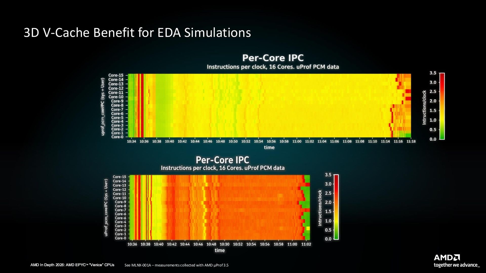
An example of one such workload is above, measuring IPC with AMD's uProf monitoring utility. With 3D V-Cache, AMD says this workload completes 40% faster at around double the instructions per clock. AMD didn't clarify which chips it was comparing or what application it was using. However, the comparison is between an EPYC fleet with and without 3D V-Cache.
Steinke says AMD is able to now move toward a single chip with Venice-X, maintaining the cache advantages in workloads like functional verification while driving the EDA workloads more sensitive to frequency. "I mentioned we have a mix of high frequency and 3D V-Cache CPUs in our data center, and that's because through Milan and Genoa, the high frequency parts were always a little higher on the frequency side," Steinke said. "You don't have that dichotomy [with Venice-X]. You can get the best of both worlds in a single CPU, and this is what we're really excited to be picking up for our own use."
AMD hasn't shared any benchmarks for Venice-X yet, but it provided some more specific HPC benchmarks comparing its high-frequency EPYC 9686F to Intel's Xeon 6980P in several HPC workloads, such as computational fluid dynamics. In AMD's testing, the 9686F was 1.6x faster in these benchmarks while running 32 fewer cores.
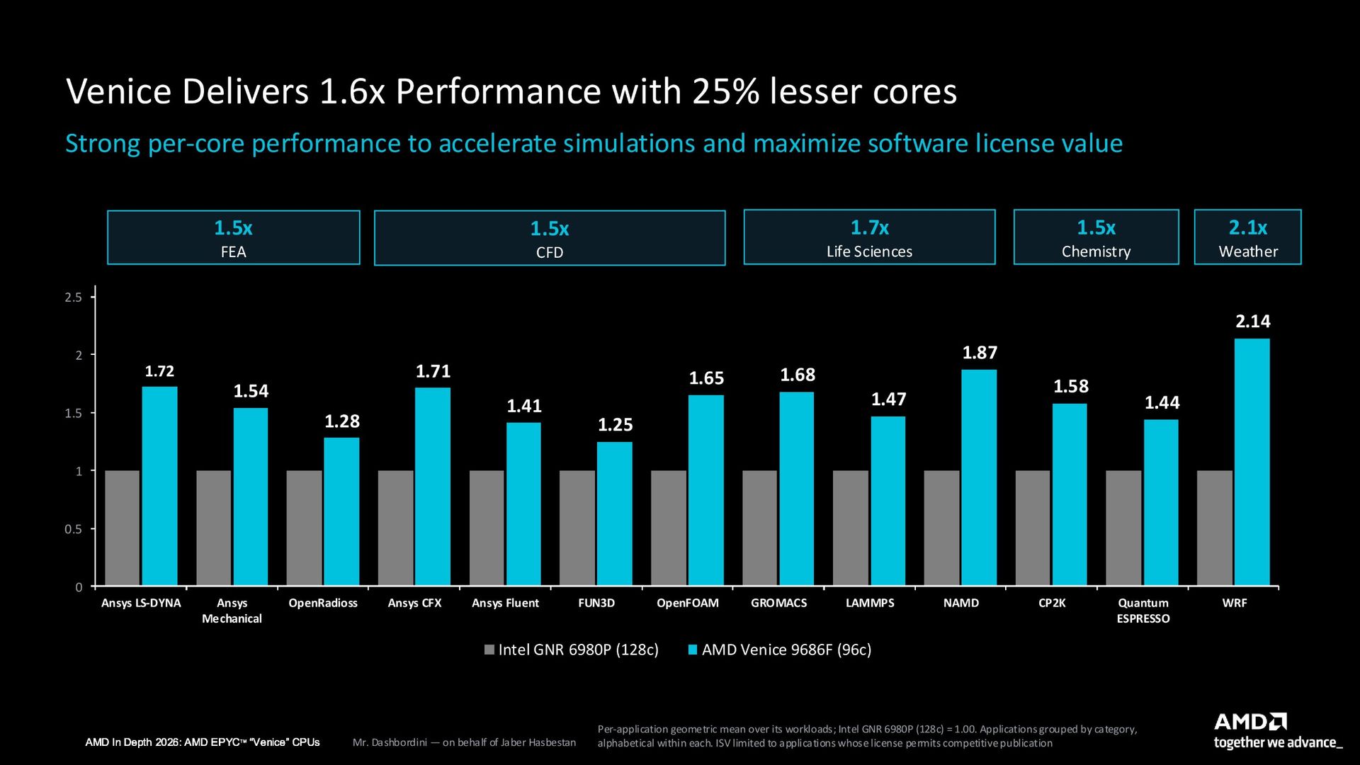
We had a chance to test the EPYC 9686F along with the dense EPYC 9996, which you can read more about in our Zen 6 EPYC Venice deep dive and benchmarking article. And indeed, the EPYC 9686F looks very impressive in some of the HPC workloads we ran.
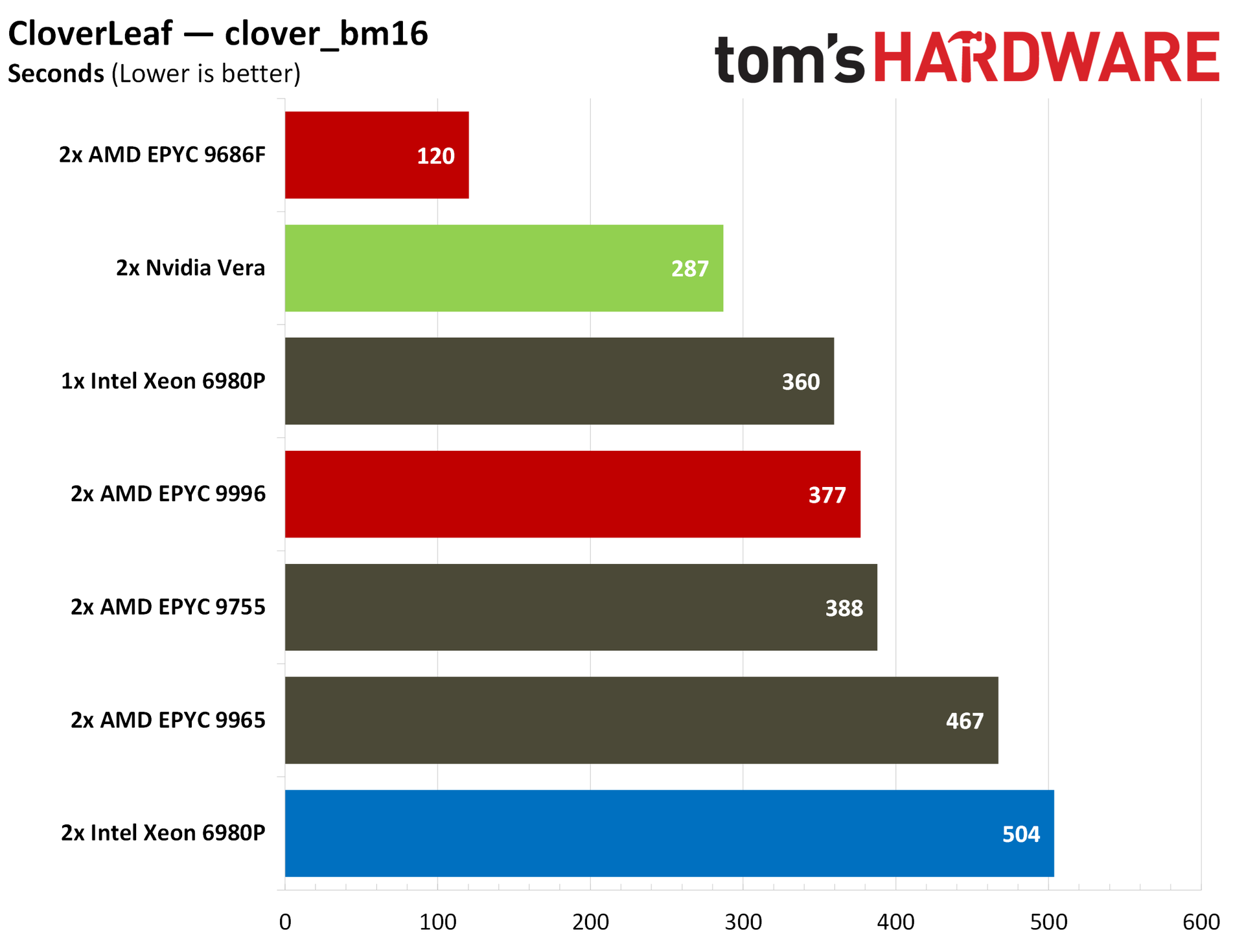
We were only able to test a 2P configuration, and as evidenced by the sole Xeon 6980P, CloverLeaf is sensitive to latency. Even then, the 2P EPYC 9686F completed the complex hydrodynamics simulation in about a third of the time as a single Xeon 6980P.
AMD says it's currently using MEXT, its AI-driven flash-as-DRAM technology, to bolster the amount of memory available for its EDA workloads. When it deploys Venice-X, Steinke says the company will continue using MEXT, which you can read more about in our recent MEXT breakdown on Tom's Hardware Premium.
Venice-X CPUs are launching in the second half of 2027, while SP7 and SP8 Venice CPUs are rolling out now. Also coming in the second half of next year is AMD's Verano, which it's pitching as an AI host node that leverages SOCAMM2 LPDDR5X memory.
正文保留英文原文,标题与摘要由机器翻译。
原文发布于 Tom's Hardware(AMD’s Venice-X maxes out family at 5.3 GHz, returning 3D V-Cache to data center after four years),标题、摘要与正文由机器翻译,术语按行业惯例统一,未经人工逐句校订。